ABOUT SILICONCIRCUITSOLUTIONS


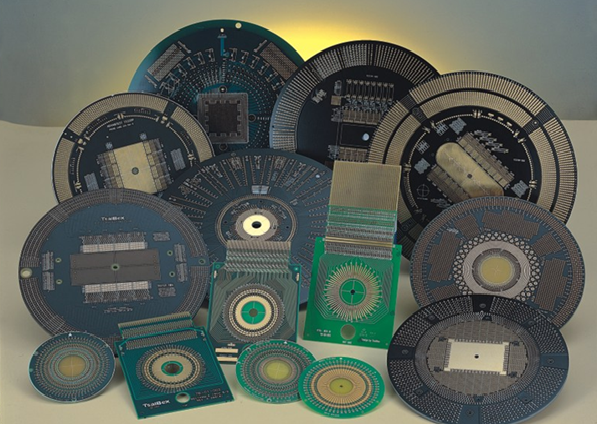
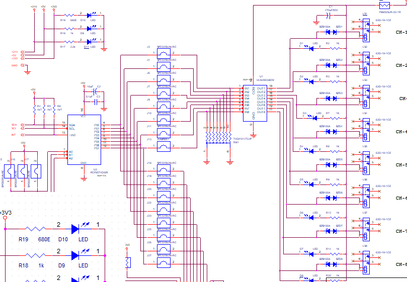
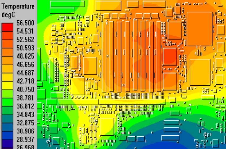
Siliconcircuitsolutions is a poineer company providing high performance IC products.siliconcircuitsolutions company , since 2017, is providing Power board PCB design,IC Packaging,PCBA Functional Test Support to costomer as per their requirment.A team of experienced Printed Circuit Board designers, specialized in IC packages supported by a simulation team performing Signal Integrity, Power Integrity and Thermal Analysis ensures all our products and boards are designed and validated to the correctness of the design

Read More
Our Services

High quality services

(IC Package Design)

PCB Layout and Schematic

Schematic & library FootprintCreations

SI & PI simulations

PROBE CARD (ATE)

Silicon Circuitsprovides complete probe card (ATE) design solution to various sector/domains of the electronics industry. We are experienced in designing and detailing of 62 layer boards with high-speed SERDES.

  • High Speed digital, Analog, Mixed and RF designs.
  • High Layer count boards : upto 62 layers
  • Impedance controlled Designs with delay matching, Stack-up and material selection.
  • DFine Pitch BGA (0.5mm), High Pin count BGA (1900+ pins).

SUBSTRATE DESIGN

Silicon Circuitsprovide substrate design service for package design technologies such as flip-chip, wire-bond, stacked-die, System-in-Package (SiP),Package-on-package (PoP), Package-in-Package (PiP), Chip-scale-package (CSP) and other vertical space transformers (MLO/MLC) meant for ATE testing applications.

  • Worked with Digital, Analog and mixed designs concepts.
  • Experience in Power DC simulation.
  • Knowledge in EMI/EMC at substrate layout level.

PCB HIGH SPEED BOARD

Silicon Circuitsprovides complete PCB design solution to various sector/domains of the electronics industry. We are experienced in designing and detailing of 36 layer boards with high-speed SERDES and over 15,000 components. Miniature PCB design with mixed-signal design which can fit in a small tube.

  • High speed digital, Analog, mixed Digital/Analog, RF designs.
  • High Layer count (36 layers), Ultra High density designs.
  • Routing and Length matching of critical signals.

SCHEMATIC AND LIBRARY FOOTPRINT CREATIONS

Silicon Circuitsknowledge in creating schematic diagrams that are easy to read while following the signal flow through the circuit. Schematics capture from hand sketches, block diagrams or Partial schematics for any of industry CAD tools.

  • Schematic Symbol&footprintcreation.
  • Capturing Hand written schematic.
  • Integration of Schematic and Layout.

SI & PI SIMULATIONS

Controlled impedance calculation – Can model diffpair and SE signals separately for loss analysis – Can analyze Xtalk for different spacing. – Can analzse signal speed that can be supported by the trace

Allegro Package SI is used for Signal net SI analysis.

Define Specification & Stack-Up Verification

Power/GND Impedance profile analysis  De-coupling Capacitors Estimation  Common-mode radiated noise (EMI)  IR drop analysis