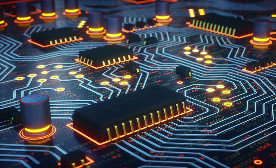
PCB HIGH SPEED BOARD
Silicon Circuitsprovides complete PCB design solution to various sector/domains of the electronics industry. We are experienced in designing and detailing of 36 layer boards with high-speed SERDES and over 15,000 components. Miniature PCB design with mixed-signal design which can fit in a small tube. Our team has experience in delivering desired outputs quickly and accurately as per specifications and guidelines
- Our extensive knowledge enables the design team to deliver the product on time with cost effective solutions
- We provide an efficient design service to our customers while taking into account all the necessary design criteria to ensure a First-Time-Right Product Design Solution.
PCB Layout Highlights
- High speed digital, Analog, mixed Digital/Analog, RF designs.
- Impedance controlled Designs with 50E, 75E, 60E, 45E, 90E and 100E Stack-up and material selection.
- High Layer count (36 layers), Ultra High density designs.
- FP creation as per IPC7351 (A,B and C) including if any customer specifications standards.
- High speed interconnects: 10 Gbps
- Critical and associated Components placement.
- Designs with Micro Vias, Blind Vias, Buried Vias and backdrill.
- Routing and Length matching of critical signals.
- High Layer count (36 layers), Ultra High density designs.
- FP creation as per IPC7351 (A,B and C) including if any customer specifications standards.
- Generating Length reports of signals.
- Gerber Setting and Fab, Assembly output Generation in 274X and ODB++ Format.
