SUBSTRATE DESIGN
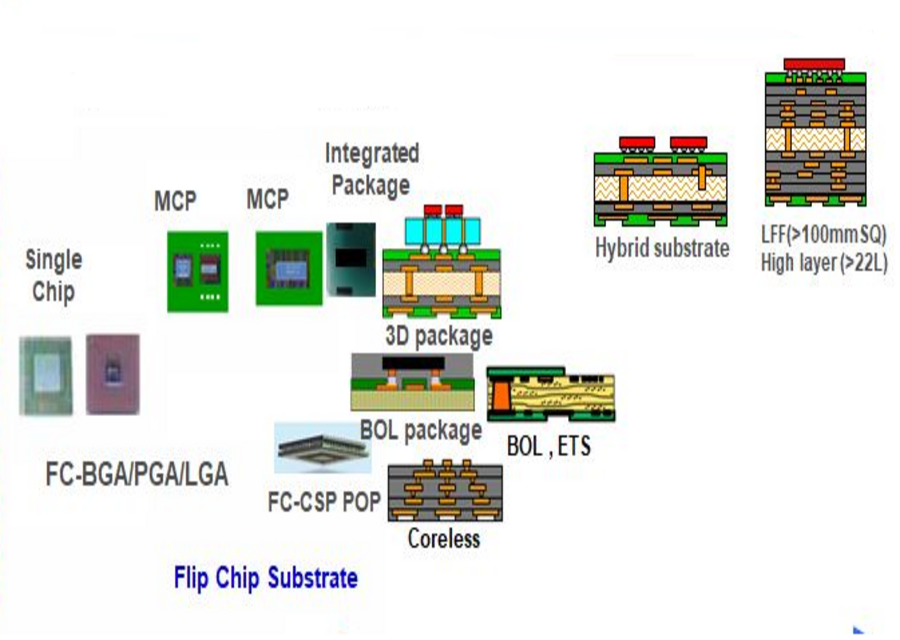
Silicon Circuitsprovide substrate design service for package design technologies such as flip-chip, wire-bond, stacked-die, System-in-Package (SiP),Package-on-package (PoP), Package-in-Package (PiP), Chip-scale-package (CSP) and other vertical space transformers (MLO/MLC) meant for ATE testing applications.
Silicon Circuits will provide MLO, MLC and coreless substrate design services from your specification and High density design with high I/O count services for multicore and coreless technology for MLO designs.
- Worked with Digital, Analog and mixed designs concepts..
- Knowledge in EMI/EMC at substrate layout level.
- Experience in Power DC simulation.
Key Specifications
- Experienced in substrate design using (Flip-Chip BGA, Wire-bond BGA,) MLO/MLC process.
- Hands on experience in Thin film (coreless) technology.
- Experienced in interposer design using expedition tool.
- Worked in many Organic substrate design with high I/O pin count with stringent PDN specifications.
- Worked in single / multiple core configuration and coreless constructions.
- Experience in handling Micro/Blind buried via PTH via technology.
- Worked with DDR, USB, P-Phy, UFS, LPDP and MIPI interfaces.
- Having fundamental understanding of Signal Integrity and Power Integrity to meet tight electrical specifications..